|
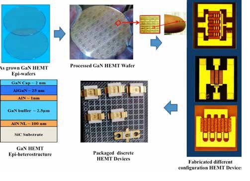
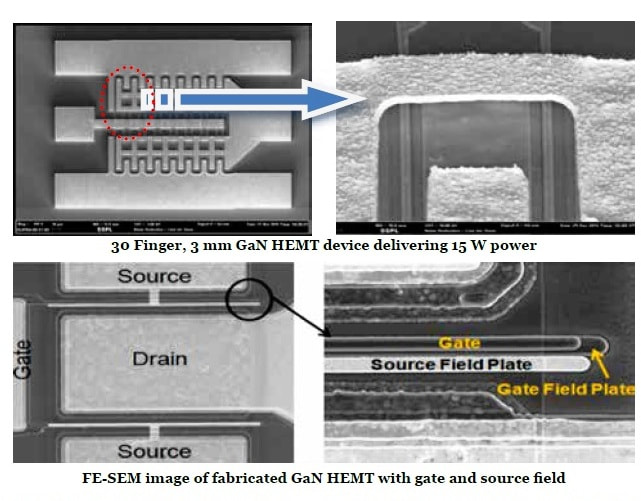
Gallium Nitride (GaN)-based High Electron Mobility Transistor (HEMT) technology is revolutionizing the modern defence RF and electronic warfare systems. The capability of AlGaN/GaN HEMT to deliver high power, high frequency, high linearity, high efficiency and high temperature performance renders it the most sought after device for applications in advanced radars, data links, satcoms, etc. Particularly for RF power applications, GaN-based HEMT technology offers a significant advantage over the existing gallium arsenide (GaAs) Monolithic Microwave Integrated Circuits (MMICs). This is primarily due to the capability of GaN devices to operate at higher voltages owing to very high breakdown fields associated with them. Additionally, the GaN devices offer much higher impedance resulting in the requirement of less complex matching networks in RF power amplifier integrated circuits. On the whole, GaN technology results in minimizing the sizes of RF ICs by a factor of ten or even higher over the competing RF technologies. Moreover, the low current operation aided with a higher efficiency results in power saving and reduced costs for cooling the system. Therefore, the GaN-based power amplifiers constitute the heart of present day transceiver (T/R) modules in AESA (Active Electronically Scanned Array) radars and communication systems. To harness the potential of this technology, a project entitled AlGaN/GaN High Electron Mobility Transistors: Material and Device Technology Development (BALRAM) was undertaken by Solid State Physics Laboratory (SSPL) as a first step towards achieving long term self-reliance in GaN-based material, high power devices/MMICs for RF applications. SSPL evolved process control and characterization methodologies, besides, timely development of facilities for (a) epi-wafer growth and characterization, (b) device simulation, (c) device fabrication and (d) DC, RF and load pull measurement etc. TECHNOLOGY DEVELOPMENT EPI-Wafer Growth Technology AlGaN/GaN hetero-structures having a two dimensional (2D) electron gas with a high electron density of ~1013 cm-2 and electron mobility of ~2000 cm-2 V-1s-1 are required for fabrication of high performance HEMT devices. A typical GaN HEMT hetero-structures consists of a multilayer hetero-epitaxial structure with strict control over composition as well as thicknesses at nanometer scale. The desired smoothness/abruptness of various interfaces at sub-nanometer level requires atomic scale control over growth process. Metal Organic Chemical Vapour Deposition (MDCVD) was selected for developing AlGaN/GaN HEMT epi-wafer growth process for its capability of scaling up for volume production and low manufacturing cost. A specially designed MOCVD reactor was established and a production worthy GaN HEMT epi-wafer growth technology was developed with sustained R&D efforts. A variety of crystalline substrate options, namely, Sapphire, SiC and Si, were explored for growing the desired epitaxial hetero-structures. However, the technology development was finally confined on SiC due to its least mismatch in lattice constant and thermal expansion coefficient with GaN. Further, a high thermal conductivity of SiC renders it most suitable for high power RF applications. The main challenges in developing the GaN HEMT material technology included achieving the desired 2D electron density and mobility with reduced dislocation density and control over impurities acting as deep electron traps. Other crucial requirements for AlGaN/GaN HEMT structure included (a) the growth of high resistivity GaN buffer layer, (b) precisely controlled 1 nm AlN exclusion layer with sharp interfaces and (c) growth of crack free AlGaN layers with step flow morphology while maintaining minimum particulate generation during growth. The indigenous GaN HEMT materials technology is matured and device quality epi-wafers are regularly produced for fabrication of Power HEMT devices and MMICs. Power HEMT Device fabrication, RF and Power Characterization Development of HEMT device fabrication technology involves a large number of unit processes that are Integrated to realize the devices with reliable and reproducible performance. The first tryst with GaN power device development involved generation of complete technological know-how ab initio. The design of Process Evaluation Vehicles (PEVs) for process development and assessment was the first step. Suitable Process Control Monitor (PCM) structures were incorporated for a strict monitoring of the fabrication process. Unit processes like formation of ohmic and Schottky metal contacts, device passivation, dry etching for contact-formation/device-isolation, plated air bridge interconnection for reduced parasitic, etc., were successfully developed and integrated. Surface passivation is one of the most important processes in GaN power HEMT technology. Optimum passivation mitigates the well-known phenomena of current collapse and I-V knee walkout. Reduced current collapse and knee walk-out results into higher output power density and long term device reliability in GaN HEMTs. The process of GaN HEMT surface passivation was optimized for current recovery and achieving high breakdown voltage. RF measurements on GaN HEMT involving high power densities require development of a thorough understanding of the complexities therein. Specialized measurement setup and methodologies were developed for this purpose. A dedicated load pull system was assembled in-house and is now being utilized regularly. As the power devices in general are oscillating and need special measurement techniques, a stabilization network was designed and fabricated to carry out the measurements. Devices fabricated with gate length of 0.4 μm and 0.25 μm demonstrated the cut-off frequencies of 33 GHz and 43 GHz, respectively. In order to achieve high performance for a given AlGaN/ GaN HEMT, features holding the maximum importance are high off-state breakdown voltage, current recovery, low gate and buffer leakage and low on-state resistance. Optimization of these features through simulations, process technology development and characterization was achieved. The main technology breakthrough included the control over breakdown voltage and knee walkout after device surface passivation through the incorporation of field plates over gates. The technology has been developed on 75 mm AlGaN/GaN on SiC substrates. Depletion mode HEMT devices with peak drain current density of 1 A/mm, peak DC trans-conductance of ~230 mS/mm and extrapolated power output of 5-6 W/mm for small periphery devices have been achieved. Post Project Developments Packaged devices with gate width of up to 2.4 mm were measured to give saturated output power of 7-8 W in S and C bands. The in-house developed bias tees have enabled the on-wafer load pull measurement of large periphery devices. The 3 mm devices in fish bone configuration could be measured to deliver a saturated output power of 15 W. The enhancement of breakdown voltage by incorporating field plates, increased the device operating voltage suitability up to 50 V from 28 V operation. Also with field plates, due to reduction in peak electric field, the availability of active electron taps between gate and drain reduces drastically resulting in minimum current collapse and knee walkout. The in-house fabricated field plated devices have successfully delivered an output RF power density ~5 W/mm at 28 V and ~10 W/mm at 50 V operations up to 6 GHz. GAN TECHNOLOGY FOR PRODUCTION Complete process sequence of GaN HEMT device fabrication has been established at GAETEC. This involved establishing all unit processes on production systems and their integration. The main challenge in transferring and establishing any process on production system is the identification of critical factors causing process drift and their control. The production process is now established to deliver discrete HEMTs in S/C band. A completely processed GaN HEMT wafer fabricated at GAETEC was released in 2017. ACHIEVEMENTS AlGaN/GaN HEMT EPI-wafers have been developed on SiC substrates, achieving mobility >2000 cm-2 V-1s1 with 2o density of ~1013 cm-2. On-wafer uniformity and process repeatability has been established over a large numbers of runs. The achieved material characteristics are comparable to the state-of-the-art in material technology. The current status of achieved power density is ~10 W/mm at 50 V and breakdown voltage greater than 150 V with field plate integration and is comparable with state-of-the-art device technology for S band applications. CURRENT STATUS AND WAY FORWARD AlGaN/GaN HEMT epi-wafers grown are being used for device fabrication. Currently further advancement in material technology is under process for growth of iron and carbon doped buffer-based heterostructures for further higher breakdown voltage operation in X band and beyond. Apart from this, growth technology is being upgraded to 4” diameter. The device process technology for 0.7 μm GaN HEMT has been stabilized and established for production at GAETEC. Using the indigenously developed 0.7 μm gate GaN HEMT discrete device, a 1.7-2.1 GHz 10 W linear power amplifier circuit is successfully designed, fabricated, assembled and tested for the desired performance. The amplifier can be used in the chain as driver amplifier to feed higher capacity power amplifiers. The development for 0.25 μm technology for X band applications is at advanced stage along with passive components. This will enable speedy development of GaN-based MMICs with applications up to X band. Source : www.drdo.gov.in 6/19/2018 05:27:58 pm
For cost effective solution, choose GaN on Si. I've found a company in Singapore providing GaN on Si epiwafers and fab process. Check out www.igssgan.com.
Reply
Leave a Reply. |
AuthorPalash Choudhari Archives
June 2021
Categories
All
|


 RSS Feed
